ナノエレクトロニクス・ナノテクノロジーの研究
メンバー: 白樫淳一
分野: ナノ・マイクロ科学、応用物理学、電気電子工学、材料工学
所属: 工学研究院
キーワード: Single-Electron Transistor、 Ultra-Small Tunnel Junction、 Quantum Point Contact、 Nanogap、 Controlled Electromigration、 Scanning Probe Microscopy、 Electron-Beam Lithography
ウェブサイト:
研究概要
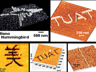
我々の研究室では、走査型プローブ顕微鏡(Scanning Probe Microscope: SPM)や電子線露光法(Electron-Beam Lithography: EBL)を利用して、ナノメートル級の超微細加工技術を新たに開発・駆使しながら、ナノテクノロジーやナノエレクトロニクスに関する研究活動を展開している。
1)リアルタイムOSによる時間確定型エレクトロマイグレーション制御システムによるナノギャップの形成技法
2)FPGAを用いた超高速フィードバック制御型エレクトロマイグレーションによる原子の移動制御
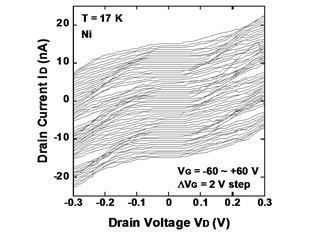
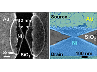
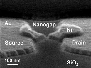
3)ナノギャップでの原子のマイグレーション現象により作製したNi系強磁性単電子トランジスタの作製
4)直並列接続型ナノギャップでの通電狭窄における構造制御パラメータについての検討
5)直列接続型ナノギャップでのエレクトロマイグレーションを利用したナノギャップの構造制御
6)ナノギャップを利用した量子ポイントコンタクトの形成と制御
7)フィードバック制御エレクトロマイグレーションによるAuナノチャネル狭窄化過程のその場AFM観察
8)薄膜グラファイト細線の通電時温度イメージング
9)ジュール加熱されたグラフェンの近赤外イメージングによるその場温度測定
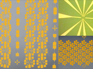
10)SPMスクラッチ法を用いたナノスケール加工のグラフェンへの適用
主要論文・参考事項
[1] R. Suda, M. Yagi, T. Watanabe and J. Shirakashi, "Formation Scheme of Quantum Point Contacts Based on Nanogaps Using Field-Emission-Induced Electromigration", J. Nanosci. Nanotechnol. 13 (2013) 883-887.
[2] S. Ueno, Y. Tomoda, W. Kume, M. Hanada, K. Takiya and J. Shirakashi, "Integration of Single-Electron Transistors Using Field-Emission-Induced Electromigration", J. Nanosci. Nanotechnol. 11 (2011) 6258-6261.
[3] T. Watanabe, K. Takiya and J. Shirakashi, "Fabrication of Planar-Type Ni/Vacuum/Ni Tunnel Junctions Based on Ferromagnetic Nanogaps Using Field-Emission-Induced Electromigration", J. Appl. Phys. 109 (2011) 07C919.
[4] W. Kume, Y. Tomoda, M. Hanada and J. Shirakashi, "Fabrication of Single-Electron Transistors Using Field-Emission-Induced Electromigration", J. Nanosci. Nanotechnol. 10 (2010) 7239-7243.
[5] J. Shirakashi, "Scanning Probe Microscope Lithography at the Micro- and Nano-Scales", J. Nanosci. Nanotechnol. 10 (2010) 4486-4494.
お問い合わせ先
東京農工大学・先端産学連携研究推進センター
urac[at]ml.tuat.ac.jp([at]を@に変換してください)
Research Activities on Nanoelectronics, Nanofabrication and Nanolithography
Research members: Jun-ichi Shirakashi PhD.
Research fields: Nano/Micro science, Applied physics, Electrical and electronic engineering, Material engineering
Departments: Institute of Engineering
Keywords: Single-Electron Transistor, Ultra-Small Tunnel Junction, Quantum Point Contact, Nanogap, Controlled Electromigration, Scanning Probe Microscopy, Electron-Beam Lithography
Web site:
Summary
OUR GROUP'S RESEARCH:
Focuses on the fabrication of nanodevices and measurement of their electronic and magnetic properties at low to room temperatures, and includes new nanofabrication techniques, magnetoresistance properties in ferromagnetic nanodevices and transport properties of electrons through Si and metallic/ferromagnetic nanostructures such as quantum dots and nanoconstrictions.
1) Nanofabrication: Scanning Probe Microscopy (SPM), Atomic Force Microscopy (AFM), SPM Local Oxidation Nanolithography, SPM Scratching Nanolithography, Electron-Beam Lithography.
2) Nanodevices: Single-Electron Transistor (SET), Ferromagnetic Single-Electron Transistor (FMSET), Ultra-Small Tunnel Junction, Ferromagnetic Tunnel Junction, Quantum Point Contact (QPC), Ferromagnetic Nanostructure, Nanogap, Nanowire.
3) Physical Properties of Interest: Single-Electron Charging Effects, Controlled Electromigration Phenomena (Voltage-Controlled, Field-Emission-Induced, FPGA-Tuned, Real-Time-OS-Controlled), Resistive Switching Effects, Magnetoresistance (MR), Anisotropic Magnetoresistance (AMR), Tunnel Magnetoresistance (TMR), Domain Wall Magnetoresistance (DWMR), Spin Injection/Current Induced Magnetization Reversal.
Reference articles and patents
[1] R. Suda, M. Yagi, T. Watanabe and J. Shirakashi, "Formation Scheme of Quantum Point Contacts Based on Nanogaps Using Field-Emission-Induced Electromigration", J. Nanosci. Nanotechnol. 13 (2013) 883-887.
[2] S. Ueno, Y. Tomoda, W. Kume, M. Hanada, K. Takiya and J. Shirakashi, "Integration of Single-Electron Transistors Using Field-Emission-Induced Electromigration", J. Nanosci. Nanotechnol. 11 (2011) 6258-6261.
[3] T. Watanabe, K. Takiya and J. Shirakashi, "Fabrication of Planar-Type Ni/Vacuum/Ni Tunnel Junctions Based on Ferromagnetic Nanogaps Using Field-Emission-Induced Electromigration", J. Appl. Phys. 109 (2011) 07C919.
[4] W. Kume, Y. Tomoda, M. Hanada and J. Shirakashi, "Fabrication of Single-Electron Transistors Using Field-Emission-Induced Electromigration", J. Nanosci. Nanotechnol. 10 (2010) 7239-7243.
[5] J. Shirakashi, "Scanning Probe Microscope Lithography at the Micro- and Nano-Scales", J. Nanosci. Nanotechnol. 10 (2010) 4486-4494.
Contact
University Research Administration Center(URAC),
Tokyo University of Agriculture andTechnology
urac[at]ml.tuat.ac.jp
(Please replace [at] with @.)